| 2004 |

|
YEAR BOOK |
University of Limerick
|
Creating structures for super-fast computers
|
New devices based on structures known as photonic crystals can address many of these problems. Photonic crystals are periodic structures that display a photonic band gap forbidding transmission of frequencies within the band gap. This photonic band gap is a characteristic due to interaction of photons with the periodic structure, which has a different refractive index from the supporting material.
In the Department of Physics and the Materials & Surface Science Institute (MSSI) at the University of Limerick, the formation of photonic crystals through the electrochemical etching of III-V semiconductors is being investigated. The mechanism that controls this process is highly dependent on the electrolyte concentration and applied voltage. Controlled modulation of the pore diameter and pore growth direction could allow the fabrication of devices based on photonic crystal structures.
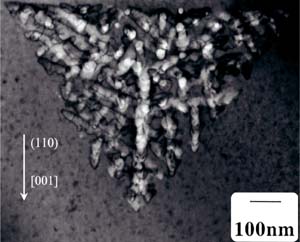
The figure shows a transmission electron micrograph (TEM) of a square based pyramidal porous domain produced in the early stages of electrochemical etching of indium phosphide (InP) in a potassium hydroxide (KOH) electrolyte. Domains originate from pits in the surface and pore growth occurs preferentially along mutually perpendicular directions corresponding to the <100> crystal directions, beneath a ~40 nm dense near-surface layer. The pore diameters, which can be controlled by varying the etching conditions, are also ~40 nm. The inter-pore wall thickness is limited by the depletion layer width, below which the holes necessary for growth are not available.
We have generated a numerical model of the growth process and it is hoped that further research will lead to regularly repeating porous patterns that, among other applications, will allow for the fabrication of three-dimensional photonic crystals.
Contact: Professor D.N. Buckley, Chair of Physics, University of Limerick;
Tel: +353-61-202902; E-mail: [email protected]